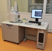
Surface structure and morphology analysis (together wit EDS elemental analysis) of conductive, semi conductive and non conductive samples.
Technical parameters
Secondary electron resolution: 3 nm, at high vacuum and 30 kV Vacc; 10 nm, , at high vacuum and 3 kV Vacc.
Backscattered electron resolution: 4 nm, at high and low vacuum and 30 k Vacc.
SEM has fully automatic vacuum system capable to achieve ≤ 1,5 x 10⁻³ Pa pressure in sample chamber, for low vacuum mode pressure is freely selectable from 10-270 Pa range.
SEM has high quality secondary and backscattered electron detectors optimised for low vacuum mode, IR-CCD camera. Bruker Quad 5040 EDS detector.
Fully motorised, large size 5-axis eucentric sample stage.
High resolution images savable in JPEG, TIFF, BMP formats.