
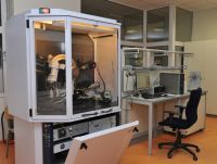
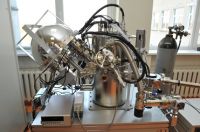
The system is used for the various composition (metals, semiconductors and oxides) and structure film synthesis using electron beam physical vapour deposition technology.
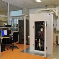
Physical vapour deposition system is designed for the deposition of metallic, semiconductive and oxide thin films/membranes synthesis using magnetron sputtering technique.
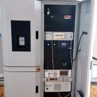
Specialized in characterization of electrical properties of materials at high temperatures and under controlled atmosphere.
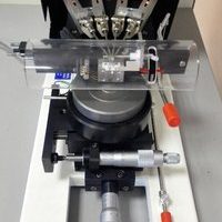
The purpose of the four point probe is to measure the resistivity of any semiconductor material.
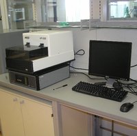
Effective instrument for performing surface hardness measurements on metals, plastics, rubbers, ceramics, and many other materials.
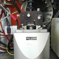
The equipment provide precision surface topography measurements on a wide variety of substrates and come with the low force frictionless pivot stylus head and a force control feedback system.
Atomic force microscopy is versatile and powerful microscopy technology for studying samples at nanoscale with high resolution.
PCTPro-2000 is a fully automated Sievert instrument for measuring gas sorption properties kinetics and thermodynamics) of materials, especially for hydrogen storage materials.
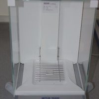
High temperature electric tube furnace for heating of samples in the air.
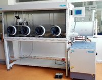
A glove box is a sealed container used to manipulate materials where a separate atmosphere is desired.
Ball milling apparatus can realize planetary ball milling process for rapid batch wise ultra fine grinding down to colloidal fineness of hard to soft materials dry or in suspensions.
It is designed to weigh small amounts of material at very high accuracies.
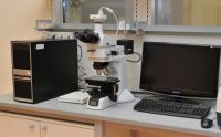
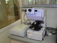
Microscope is designated for the optical investigation of magnified (up to 1000x) objects which are not visible with eye.
Equipment is used for the non-destructive analysis of all types of samples including powders and thin films.
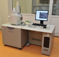
Surface structure and morphology analysis (together wit EDS elemental analysis) of conductive, semi conductive and non conductive samples.
Equipment is designed for measurement of nitrogen, oxygen, and hydrogen amount in a wide variety of metals and other inorganic materials, employing the inert gas fusion principle. Also equipment has possibility to determine gas release from surface contaminated sample which is achieved by pre-treatment of sample with various gas mixtures prepared by special gas premixer.
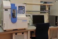
Bulk elemental analysis of metals, alloys and other substances and for qualitative and quantitative depth profiling of thin film/layer systems with conductive and non-conductive layers, and for detecting changes in chemical composition of sample surface compared to the subsurface material.
Equipment is designated for the XPS analysis of various samples (including thin films and nanopowders) for the determination of elemental and chemical composition.
Equipment is designated for the Auger electron spectroscopy and Auger electron microscopy analysis of sample surfaces, nanometric particles at the surface and other nanometric features including interface between thin films and their substrate.

Particularly precise (6 nm spatial resolution, 2-3 atomic monolayers volume (depth) resolution) identification of surface and volumetric (up to 1-2 μm depth) derivatives, determination of elemental composition, obtainment of chemical (bond) information. Problems and limitations can be found when testing dielectric specimens in particular.
Quick, low-precision (spatial accuracy about 2-4 millimeters, profiling depth precision tens-hundreds nanometers) qualitative and quantitative elemental composition analysis. Ability to perform depth profiling, composition control and comparison between surface and deeper layers.
Using inert gas fusion principle we carry out an accurate analysis of even very small amounts of nitrogen, oxygen and hydrogen in various materials. Measurements require up to 1-2g of the test substance that is melted at high temperature during the analysis and the amount of gas released is measured.
Qualitative and quantitative measurements of optical bandwidth in the spectral range of 163-1100 nm.
Variable pressure scanning electron microscope can be used to analyze both conductive and dielectric samples. It is also possible to analyze biological objects with certain limitations. SEM resolution at 30 kV accelerating voltage is 3 nm, while at 3 kV accelerating voltage, 8-10 nm resolution is achieved. We can create images with both secondary and reflective electron detectors, so there is a possibility to separately highlight the unevenness of sample morphology, elemental composition, and extract detailed pseudo 3D images.
Quantitative and qualitative determination of the elemental composition of the sample by detecting chemical elements from Boro5 to Americio95 at the selected point (spatial resolution 1-2 μm, depending on the measurement conditions, information is obtained from 0.5-2 μm depth). It is also possible to map the distribution of individual chemical elements in the sample area.
All crystalline phases in the sample can be determined by one measurement. There are also extended possibilities for diffraction measurements at the same time controlling the ambient temperature (from liquid nitrogen to 1600 oC) and the surrounding environment (high vacuum can be used or the desired amount of gas (suitable for many gases) up to a maximum pressure of 5 bar).
Ability to perform sample analysis using a high-quality optical microscope with the ability to store images in high-resolution photos. Microscope enhancement is selected between 100, 200, 500 and 1000 times. The photos are made with the NIKON DSF-1Fi digital camera specially designed for optical microscopy with a resolution of 2560 x 1920 pixels.
The system is used for the various composition (metals, semiconductors and oxides) and structure film synthesis using electron beam physical vapour deposition technology.
Physical vapour deposition system is designed for the deposition of metallic, semiconductive and oxide thin films/membranes synthesis using magnetron sputtering technique.
Specialized in characterization of electrical properties of materials at high temperatures and under controlled atmosphere.
The purpose of the four point probe is to measure the resistivity of any semiconductor material.
Effective instrument for performing surface hardness measurements on metals, plastics, rubbers, ceramics, and many other materials.
The equipment provide precision surface topography measurements on a wide variety of substrates and come with the low force frictionless pivot stylus head and a force control feedback system.
Atomic force microscopy is versatile and powerful microscopy technology for studying samples at nanoscale with high resolution.
PCTPro-2000 is a fully automated Sievert instrument for measuring gas sorption properties kinetics and thermodynamics) of materials, especially for hydrogen storage materials.
High temperature electric tube furnace for heating of samples in the air.
A glove box is a sealed container used to manipulate materials where a separate atmosphere is desired.
Ball milling apparatus can realize planetary ball milling process for rapid batch wise ultra fine grinding down to colloidal fineness of hard to soft materials dry or in suspensions.
Microscope is designated for the optical investigation of magnified (up to 1000x) objects which are not visible with eye.
Equipment is used for the non-destructive analysis of all types of samples including powders and thin films.
Surface structure and morphology analysis (together wit EDS elemental analysis) of conductive, semi conductive and non conductive samples.
Equipment is designed for measurement of nitrogen, oxygen, and hydrogen amount in a wide variety of metals and other inorganic materials, employing the inert gas fusion principle. Also equipment has possibility to determine gas release from surface contaminated sample which is achieved by pre-treatment of sample with various gas mixtures prepared by special gas premixer.
Bulk elemental analysis of metals, alloys and other substances and for qualitative and quantitative depth profiling of thin film/layer systems with conductive and non-conductive layers, and for detecting changes in chemical composition of sample surface compared to the subsurface material.
Equipment is designated for the XPS analysis of various samples (including thin films and nanopowders) for the determination of elemental and chemical composition.
Equipment is designated for the Auger electron spectroscopy and Auger electron microscopy analysis of sample surfaces, nanometric particles at the surface and other nanometric features including interface between thin films and their substrate.


